
Semiconductor & MEMS Process Services
MEMS
Foundry Service
Process services on 4-, 6-, and 8-inch silicon or glass wafers
Scroll Down
Semiconductor & MEMS Process Services
Process services on 4-, 6-, and 8-inch silicon or glass wafers
Core Process Services
We provide front-end foundry services for semiconductor and MEMS device fabrication.
Manufacturing Flow
A systematic foundry process from design request to finished product shipment
Analysis of customer requirements, process feasibility review, and optimal process proposals
Chrome or emulsion mask fabrication. Precision lithography masks for high-resolution patterning
Customer-supplied or in-house processed materials
Core processes including photolithography, etching, deposition, and plating
Wafer inspection and shipment with a quality report
Product Portfolio
We supply key devices for semiconductor and MEMS packaging, from design through fabrication.

SOI Wafer
Silicon-on-InsulatorA specialized semiconductor substrate with an insulating (oxide) layer between silicon layers that blocks leakage current and significantly improves operating speed and power efficiency

TSV Interposer
TSV InterposerA through-silicon via interposer for heterogeneous chip integration. Supports high-speed signal transmission with a fine pad pitch and low parasitic resistance

TGV Interposer
TGV InterposerA next-generation high-performance packaging substrate that connects the semiconductor chip to the main board by forming fine vertical vias in a glass substrate and filling them with metal

Copper Post Bump
Copper Post BumpA next-generation interconnect terminal that uses copper posts to significantly improve signal transmission speed and fine-pitch capability
Test Element Group
We provide Test Element Group wafers and design files for process verification.

TEG layout DXF files for each product, including SOIWA, CPBT, TGVI, and TSVI, to support design verification
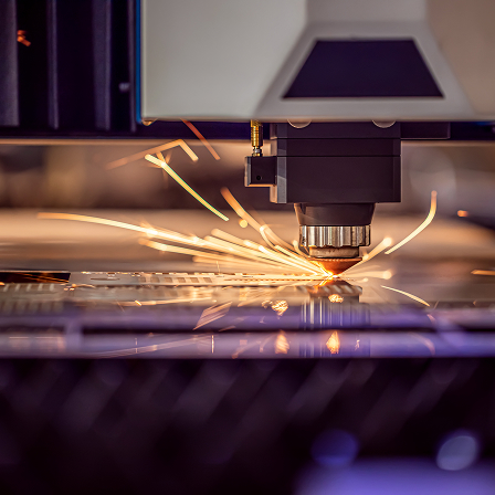
Includes electrical test structures for monitoring process variables such as resistance, contacts, and via chains. Real-time tracking of process stability
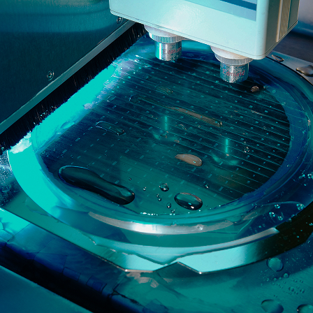
TEG structures can be customized to customer specifications, including proposals to optimize die area utilization

Wafer-level electrical measurement results and yield analysis reports, supporting a feedback loop for process optimization
Contact
Headquarters : 10F, Room 1015, 614 Dongtangiheung-ro, Hwaseong-si, Gyeonggi-do, Republic of Korea (Yeongcheon-dong)
FAB & Research Institute : Room 81410, 1st Comprehensive Research Building, 2066 Seobu-ro, Jangan-gu, Suwon-si, Gyeonggi-do, Republic of Korea
Copyright © EPG All rights reserved.
Designed by Website.co.kr