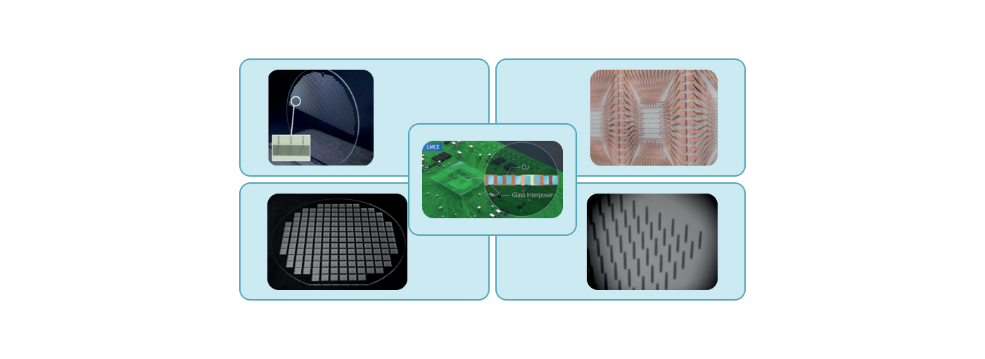
TGV interposer

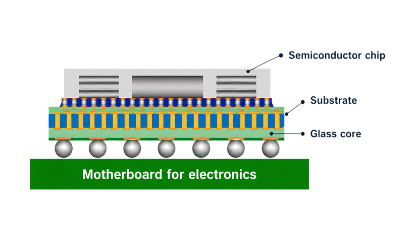
Through-glass via (TGV) technology enables glass substrates to be used for 3D integration
in applications such as RF modules and sensor packaging.
EPG's TGVi® technology provides TGV substrates for semiconductor packaging and a wide range of advanced packaging applications.
Through Glass Vias
for Semiconductor Packaging
Through-Glass Vias
for Semiconductor Packaging
TGV substrates offer excellent electrical insulation, dimensional
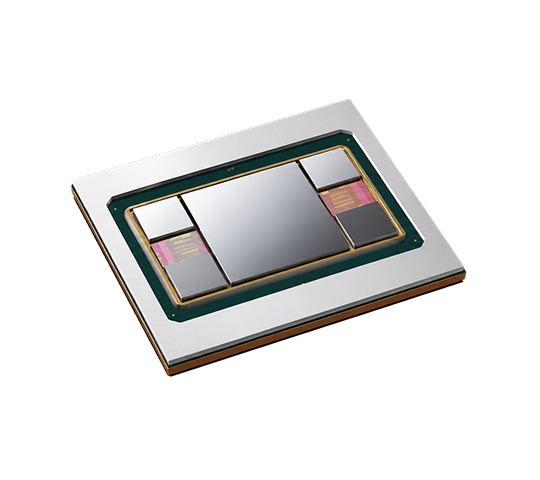
stability, and RF performance, making them well suited for advanced semiconductor packaging.
TGV technology enables high-density vertical interconnections through glass substrates and can be applied to RF devices, sensors, MEMS, and various 3D integration applications.
- Glass material
- Boro 33, D263, AS87, Eagle XG, Quartz....
- Size
- Wafer: φ100mm, φ150mm, φ200mm
- Thickness
- 0.3mmT ~ 1mmT
- Hole type
- Through via, Blind via
- Hole shape
- Straight
- Hole diameter
- Φ25um ~
- Pitch
- Min. hole dia x 2
TGV Applications and Process Overview